PCB Designing Mastery
From schematic design to professional PCB layout - master the art of printed circuit board design with industry-standard techniques
Circuit Fundamentals
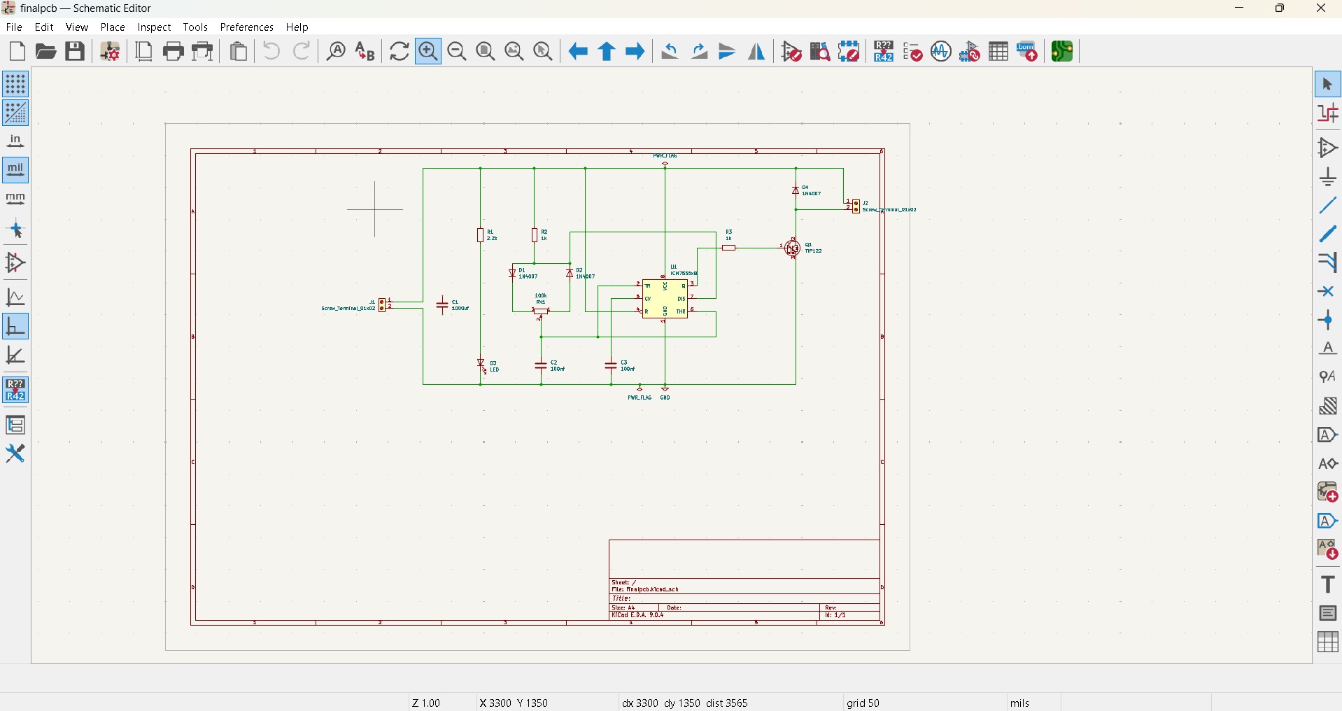
AC to DC Converter Schematic
- Designed schematic for a basic AC to DC converter circuit
- Component selection and electrical specifications analysis
- Circuit topology understanding and power flow concepts
- Schematic symbol placement and electrical connections
PCB Basics & Fundamentals
- PCB layers: substrate, copper, solder mask, and silkscreen
- Understanding traces: width, spacing, current capacity
- Vias: through-hole, blind, and buried via applications
- Component footprints and pad design considerations
- Design rules and manufacturing constraints
Real-world Applications: Discussed practical applications of PCB in various industries, best design practices for reliability and manufacturability, and industry standards for professional PCB development.
Layout Implementation
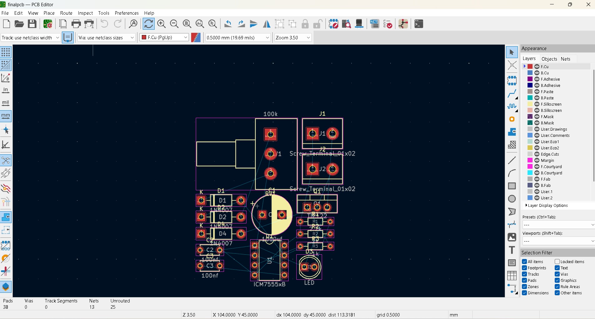
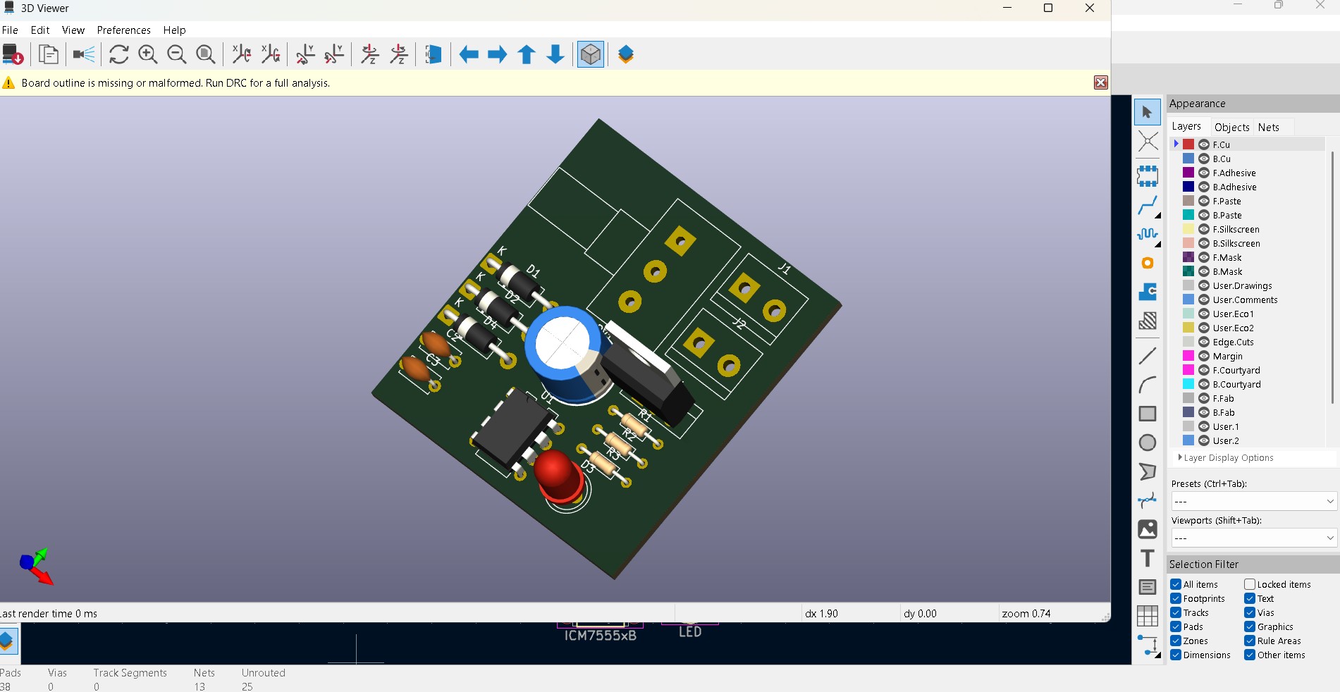
AC to DC Converter Layout
- Converted schematic to PCB layout using professional software
- Board outline creation and mechanical constraints definition
- Layer stack-up planning for power and signal integrity
- Netlist import and component footprint assignment
Component Placement & Routing
- Strategic component placement for optimal performance
- Manual and auto-routing techniques for efficient connections
- Power and ground plane implementation strategies
- DRC (Design Rule Check) error resolution methods
- Signal integrity and noise reduction techniques
Independent Practice: Students worked on layout tools independently under guidance, gaining practical experience with industry-standard PCB design software and real-world design challenges.
Motor Control Project
DC Motor Speed Controller Schematic
- Designed DC motor control circuit from concept to completion
- Motor driver IC selection and integration techniques
- PWM control signal routing and microcontroller interface
- Protection circuits: flyback diodes and current limiting
- Power supply design and thermal management
Layout Design & Implementation
- Converted schematic to physical PCB layout
- Strategic component placement for high-current paths
- Thermal management through copper pours
- Manufacturing documentation preparation
- Final design verification and testing procedures
Knowledge Consolidation: Cleared doubts related to layout design principles, simulation techniques, and real-world implementation challenges. Comprehensive review covering manufacturing processes, cost optimization, and industry best practices.